


封装品种
- TO 系列
Production Overview
Plastic Transistor Outline packaging (TO) is a principal package using TH or SMD technology. It is widely used in low cost and manual applications. CDPT offers TO251(IPAK), TO252(DPAK), TO263(DDPAK), TO220 ,TO262,TO220F,TO247 ,TO3P packages.
Application
Transistor Outline packages are considered one of the most established industry standard packages. TO is commonly used power supplies, converters and power motor controls, Hand-held Instruments battery powered consumer products,etc.
Features
* JEDEC standard compliant or reference
* Wide choice of pad sizes to meet die size per customer lead frame design capability
* Pb-free process ready and Green Molding Compound
Reliability Test Standards
The test criterion is zero defect out of 77 sampling units.
JEDEC Precondition :J-STD-20/JESD22-A113
| Temp/Humidity Test | 85°C/ 85% RH, JEDEC 22- A101 |
| Pressure Cooker Test | 121°C/ 100% RH/ 15 PSIG, JEDEC 22- A102 |
| Temp Cycle Test | -65 ~ 150°C, JEDEC22-A104 |
| High Temp Storage Test | 150°C, JEDEC 22- A103 |
| High Accelerated Stress Test | 130°C/ 85% RH/ 33.5 PSIA, JEDEC 22- A110/A118 |
Design Rule
Minimum Ink Size: 20mil (500 um) diameter or non-ink with wafer mapping
Maximum Ink Height: 1mil(25um)
Minimum Sawing street width: 2.4mil (60um)
Wafer Thickness: Back grinding is required if the thickness exceeds CDPT spec.
| Pkg type | Pkg size | Wafer thickness |
|---|---|---|
| TO | All | Min4mil (100 um) |
| If that is asked to use soft solder for the die attachment, the wafer can not be backgrinding. | ||
Wire Bond Rule
现有能力
| Wire Bonding | Gold Wire | Copper Wire | AL Wire | AL ribbon |
|---|---|---|---|---|
| Wire Diameter | 0.7~2mil(18~50µm) | 0.8~1.5mil(20~38µm) | 5~20mil(125~500µm) | 20*3mil~80*10mil |
| Min BPO | 40*40µm | 60*60µm | 490*430µm | \ |
| Min BPO Pitch | 45µm | 70µm | 560µm | \ |
| Max wire length | 5000µm | 5000µm | \ | \ |
| Min wire length | \ | \ | 200µm | \ |
Package Outline
| PKG TYPE | Lead count | Lead Pitch | Lead Width | LeadThickness | BD | POD |
|---|---|---|---|---|---|---|
| TO-251D-3L | 3 | 2.186 | 0.72 | 0.47 | DOWN | DOWN |
| TO-252-2L | 2 | 2.186 | 0.72 | 0.47 | DOWN | DOWN |
| TO-251Q-3L | 3 | 2.186 | 0.72 | 0.47 | DOWN | DOWN |
| TO-251J-3L | 3 | 2.24 | 0.56 | 0.46 | DOWN | DOWN |
| TO-3P | 3 | 5.45 | 0.80 | 0.50 | DOWN | DOWN |
| TO-247 | 3 | 5.436 | 1.16 | 0.59 | DOWN | DOWN |
| TO-220-2L | 2 | 5.08 | 0.70 | 0.45 | DOWN | DOWN |
| TO-220-3L | 3 | 2.54 | 0.70 | 0.45 | DOWN | DOWN |
| TO-262-3L | 3 | 2.54 | 0.76 | 0.47 | DOWN | DOWN |
| TO-263-2L | 2 | 2.54 | 0.76 | 0.47 | DOWN | DOWN |
| TO-220F-2L | 2 | 5.08 | 0.70 | 0.45 | DOWN | DOWN |
| TO-220F-3L | 3 | 2.54 | 0.70 | 0.45 | DOWN | DOWN |
| TO-220FQ-3L | 3 | 2.54 | 0.76 | 0.46 | DOWN | DOWN |
Packing & Shipping
Tube
| PKG TYPE | Lead count | QTY/Tube | Tube/inner Box | QTY/Outer Box |
|---|---|---|---|---|
| TO251 | 3 | 75 | 120 | 36000 |
| TO252 | 2 | 75 | 120 | 36000 |
| TO262 | 3 | 50 | 40 | 8000 |
| TO263 | 3 | 50 | 40 | 8000 |
| TO220 | 2/3 | 50 | 40 | 8000 |
| TO220F | 2/3 | 50 | 40 | 8000 |
| TO3P | 3 | 30 | 20 | 3000 |
| TO247 | 2/3 | 30 | 20 | 3000 |
Carrier Tape
| PKG TYPE | Lead count | Tape Width | Reel Diameter | QTY/Reel | QTY/Outer Box |
|---|---|---|---|---|---|
| TO252 | 2 | 20mm | 13" | 2500 | 25000 |
| TO263 | 2/3 | 24mm | 13" | 800 | 8000 |
- IPM 系列
| PKG TYPE | Lead count | PIC |
|---|---|---|
| DIP-23E-W/DG | 23 | 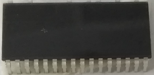 |
| DIP-23H-W | 23 | |
| SOP-23H-W/DG | 23 | 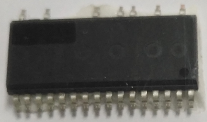 |
| DIP-24H-TG/DG | 24 | 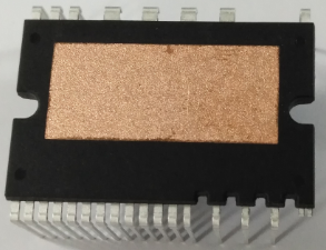 |
| DIP-25A-DG/W | 25 | 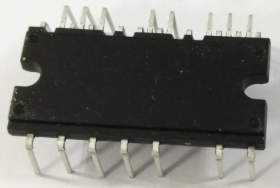 |
| DIP-27H-TG | 27 | 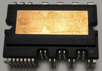 |
| SOP-27H-TG | 27 | |
IPM Packing & Shipping
| PKG TYPE | Lead count | QTY/Tube | Tube/inner Box | QTY/Outer Box |
|---|---|---|---|---|
| DIP23 | 23 | 15 | 20 | 2400 |
| SOP23 | 23 | 15 | 16 | 1920 |
| DIP24 | 24 | 12 | 5 | 480 |
| DIP25 | 25 | 13 | 20 | 2080 |
| DIP27 | 27 | 10 | 6 | 480 |
| SOP27 | 27 | 22 | 50 | 8800 |
可靠性实验能力
分立器件 试验项目 &试验条件&判定标准
| 试验项目 Test Item | 试验条件 Test Condition |
参考标准 Reference document | 选样数 Sample size | 判断标准 (A/R) |
|---|---|---|---|---|
| 高压蒸煮试验 AC(Autoclave) | 121 ℃, 29.7 psi, 100% RH, 96hrs | JESD22-A102 | 22/45/77 | 0/1 |
| 高加速老化试验 HAST(Highly Accelerated Stress Test) | TA =130℃, 85% RH, 230Kpa, Vds=80%Spec(42V max) 96hrs | JESD22-A110 | 22/45/77 | 0/1 |
| 高温反偏试验 HTRB(High Temperature Reverse Bias) | TJ = 150℃/specified TJ(max),Vds=80%Spec 1000Hrs | JESD22A-108 AEC-Q101 | 22/45/77 | 0/1 |
| 高温栅极反偏试验 HTGB(High Temperature Gate Bias) | TJ = 150℃/specified TJ(max),Vgs=100%Spec 1000Hrs | JESD22A-108 AEC-Q101 | 22/45/77 | 0/1 |
| 高温高湿偏压 H3TRB(High Humidity, High Temperature Reverse Bias) | 85℃;85% RH; Vgs=80%spec 100V MAX,1000Hrs | AEC -Q101 JESD22A-101 | 22/45/77 | 0/1 |
| 恒温恒湿实验 THT(Temp/Humidity Test) | Ta = 85℃ 85%RH | JESD22-A101 | 22/45/77 | 0/1 |
| 高温存储试验 HTSL(High Temperature Storage) | TA=150℃,1000Hrs | JESD22-A103&A113 | 22/45/77 | 0/1 |
| 不偏压高速老化 UHAST (Unbiased Temperature/Humidity) | 130℃;85% RH ; 96hrs | JESD22A-118 | 22/45/77 | 0/1 |
| 温度循环 TC(Temperature Cycling) | -65℃~+150℃, Tdwell ≥10min,500 cycles | JESD22-A104 | 22/45/77 | 0/1 |
| 耐焊接热 RSH(Resistance to Solder Heat) | SDM: A111 or J-STD-020 THMD: B1016 | JESD22A-A113 J-STD-020 | 10 | 0/1 |
| 易焊性 SD(Solder ability) | 245℃,5s,solder area>95% | JESD22-B102 | 10 | 0/1 |
测试能力
CDPT provides a complete range of Power device testing services including final testing and system level testing.
CDPT provide customers with a full range of test platforms covering test style of DC/EAS/ISO/RG/IFSM/IRSM.
| Tester Models | Manufacturer | Specifications | Test style | |
|---|---|---|---|---|
| STA2100 | STATEC | Korea | 2000V/100A | DC |
| im1020 | STATEC | Korea | 1000V/20A | DC |
| DTS1000 | JUNO | Japan | 1000V/20A | DC |
| 351-TT | TESEC | Japan | 2000V/50A(200A) | DC |
| ITC55100 | ITC | American | Vdd max 150V;Peak I max 150A | EAS |
| EAS2100/imEAS100 | STATEC | Korea | Vdd max 100V ;Peak I max 100A; L=0.01~79.9MH | EAS |
| TOS9201 | KIKUSUI | Japan | Dc max 6KV; Ac max 5KV | ISO |
| RG2009 | STATEC | Korea | RG:0.5-50Ω;CG:400pF ~ 20nF | RG |
| E4980AL | AGLIENT | China.Beijing | 1.0000aF-999.9999EF;1.0000aΩ-999.9999EΩ | RG |
| PIF6000 | POWORLD | China.Taiwan | VF:1mV~8000mV;IFS:0~200A | IFSM |
| SSG6000 | POWORLD | China.Taiwan | IR:0.1A~5.0A; VR:5.0V~300.0V | IRSM |
技术优势
◇ IPM功率模块封装测试
◇ TO功率器件封装测试
◇ MEMS加速度计、陀螺仪、压力计、磁力计传感器封装
◇ LED驱动电路封装测试
◇ MCM(MCP)多芯片封装
◇ CSP封装
◇ 纯锡电镀无铅封装
◇ 无引线扁平封装
◇ 应用于IC、功率模块的铜线键合
◇ 应用于IC封装的银合金线键合
◇ 应用于POWER器件的CLIP装片键合
